

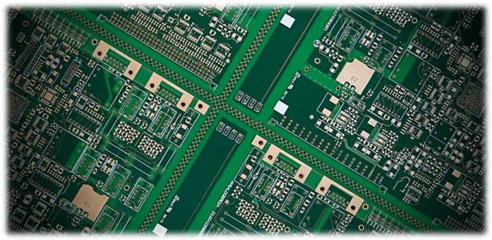
When you think about the rapidly growing world of the Internet of Things (IoT), your mind probably jumps to smart thermostats, wearable health monitors, or intelligent appliances. But behind the sleek interfaces and impressive connectivity lies a foundational component that often goes unnoticed: the HDI Printed Circuit Board (PCB). Without it, the compact design, fast processing, and high reliability of IoT devices wouldn’t be possible. In this article, you’ll uncover why HDI PCBs are the unsung heroes of IoT and how companies like Pcb-Togo Electronic, Inc are enabling innovation at the micro level.
What Is an HDI Printed Circuit Board?
HDI stands for High-Density Interconnect, and it refers to a type of PCB that offers higher wiring density per unit area compared to traditional PCBs. That means you can cram more functionality into a smaller space—exactly what’s needed in modern-day IoT devices.
Unlike standard PCBs that may have a few layers and simple via designs, HDI PCBs employ microvias, blind and buried vias, and multiple layers to create dense interconnections. This design allows for high-speed signal transmission and better overall performance. In simpler terms, HDI PCBs allow your smartwatch or smart home hub to be small, powerful, and efficient—all at once.
Why HDI PCBs Are Critical in IoT Devices
As an IoT developer, engineer, or enthusiast, you know that space is always a constraint. Devices need to be smaller, more efficient, and more powerful. That’s where HDI PCBs shine:
1. Miniaturization with Maximum Power
IoT devices thrive on compactness. Whether it’s a fitness tracker or a smart refrigerator, there’s limited real estate for electronics. HDI PCBs provide a solution by allowing more components to be integrated into fewer layers, saving space while delivering robust functionality.
2. Faster Signal Transmission
Because of their unique design, HDI PCBs offer shorter signal paths, which translates to faster communication between components. In a world where milliseconds matter—such as in healthcare monitoring devices or industrial sensors—this speed can make a significant difference.
3. Better Reliability and Signal Integrity
With more interconnects and shorter distances between them, HDI PCBs reduce electromagnetic interference and improve signal integrity. This reliability is crucial in critical applications like medical IoT or smart automotive technologies.
4. Energy Efficiency
Low power consumption is a cornerstone of IoT technology. Devices are expected to run on batteries for months or even years. HDI PCBs help by reducing the length of copper traces and minimizing power loss, thus extending battery life.
Real-World Applications
You’re probably already benefiting from HDI PCBs without even realizing it. Here are just a few examples of where you might find them:
- Wearables: Smartwatches, fitness bands, and health monitors rely on HDI PCBs for their compact design and real-time data processing.
- Smart Home Devices: Thermostats, security systems, and voice assistants use HDI technology to manage complex functionalities in a small form factor.
- Medical Devices: Portable diagnostics and monitoring equipment need high reliability and compactness—two things HDI PCBs provide effortlessly.
- Industrial IoT: In factory automation and predictive maintenance, HDI PCBs enable robust data processing and real-time analytics in edge devices.
- Automotive Sensors: As vehicles become smarter, the need for compact and reliable electronic components becomes more critical.
The Role of Manufacturers: Why Choose Pcb-Togo Electronic, Inc
If you’re in the business of creating IoT devices, choosing the right PCB manufacturer can make or break your product. This is where Pcb-Togo Electronic, Inc stands out. With years of experience in crafting HDI printed circuit board, they offer precision, reliability, and customization that developers trust.
Pcb-Togo Electronic, Inc specializes in:
- Custom HDI PCB fabrication
- Quick turnaround times
- Support for complex multilayer designs
- Compliance with global quality standards
Their team works closely with clients from concept to production, ensuring your HDI PCB is not only functional but optimized for performance and cost. Whether you’re a startup creating your first smart gadget or a large-scale manufacturer needing bulk production, Pcb-Togo Electronic, Inc provides scalable solutions.
If you have questions or are ready to take your IoT product to the next level, don’t hesitate to contant us through their official website or customer support team. A consultation could be the first step toward building a better, smarter device.
HDI PCB vs. Traditional PCB: A Quick Comparison
| Feature | Traditional PCB | HDI PCB |
| Layer Count | 1-4 layers (commonly) | Up to 16+ layers |
| Via Type | Through-hole vias | Microvias, blind/buried vias |
| Space Efficiency | Moderate | Very High |
| Signal Speed | Slower | Faster |
| Cost | Lower for basic designs | Higher upfront but better ROI |
| Application | General electronics | IoT, wearables, medical devices, etc. |
While HDI PCBs may be costlier to manufacture, the benefits in performance, size, and efficiency make them ideal for cutting-edge applications.
Final Thoughts:
As IoT continues to evolve—ushering in smarter cities, automated industries, and interconnected healthcare—the role of HDI PCBs will only grow more prominent. They’re not just circuit boards; they’re the nerve centers of tomorrow’s technology.
By integrating high-density interconnect solutions, you ensure that your devices remain competitive, efficient, and ready for the future. Companies like Pcb-Togo Electronic, Inc are at the forefront of this innovation, providing you with the tools to build smarter, smaller, and more reliable electronics.
So the next time you marvel at a smart gadget’s performance or design, remember there’s an HDI Printed Circuit Board inside—working silently but powerfully. And when you’re ready to create the next big thing in IoT, make sure to contant us and bring your vision to life with industry-leading PCB solutions.
